
This article reviews the theory of the Wien Bridge Oscillator. Written to support his own practical projects by Basin Street Design.
Here is the famous Wien Bridge oscillator circuit [1]. This picture is one shamelessly stolen from somewhere on the interwebs and modified for my purposes:
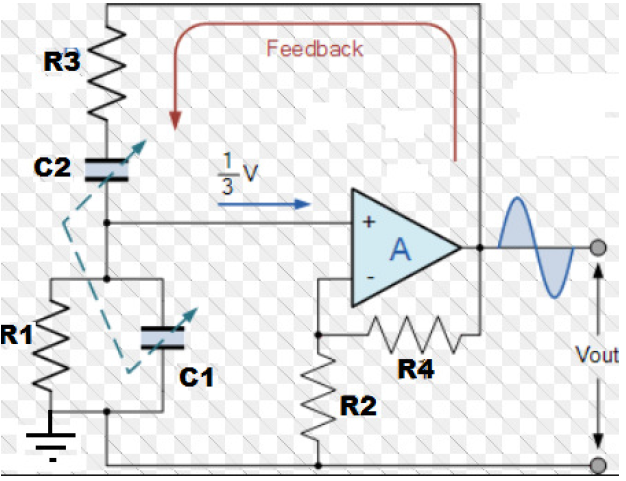
The oscillator operates by sending part of its output through the RC network (R1, R3, C1, C2) back to the non-inverting input of the op-amp (V+). The gain of the op-amp, programmed by the resistors R2 and R4, recovers the signal level lost so that the loop gain is exactly unity. Variable frequency is indicated by varying C1 and C2 on a common shaft but could just as easily be produced instead by varying R1 and R3 on a common shaft.
Simply put, the amplifier amplifies its own output. It can be shown that, ideally, the amplifier needs three things to oscillate:
– a feedback filter that prefers only one frequency above all others.
– zero time delay (phase shift) through that filter at that frequency.
– an exact gain to overcome the attenuation of the signal through said filter. In the example a gain of exactly 3 to compensante the feedback attenuation (1/3).
1. Feedback Filter
This section shows the frequency response of the feedback filter used, which is the usual series RC and parallel RC network. The fact this filter is bandpass meets the frequency-selectivity condition written above.
1.1 Transfer Function
First, I will derive the fraction of output signal to be found at the midpoint of the RC network (V+) when at resonance. For now I will assume that all component values are separate and distinct. It is found in the same way as a conventional voltage divider. The transfer function at the non-inverting input of the op-amp is the ratio of the impedance from that point to ground divided by the sum of impedances from the source to ground. In this case and using the Laplace expressions for capacitive reatance, 1/sC, this fraction is:
\begin{equation} \cfrac{V_+}{V_{out}} = \cfrac{\cfrac{\cfrac{1}{sC_1}R_1}{\cfrac{1}{sC_1}+R_1}}{\cfrac{\cfrac{1}{sC_1}R_1}{\cfrac{1}{sC_1}+R_1}+\cfrac{1}{sC_2}+R_3} \end{equation}
Previous equation can be simplified as follows:
\begin{equation} \cfrac{V_+}{V_{out}} = \cfrac{\cfrac{s}{R_3C_1}}{s^2+\left(\cfrac{1}{R_3C_1}+\cfrac{1}{R_3C_2}+\cfrac{1}{R_1C_1}\right)s+\cfrac{1}{C_1C_2R_1R_3}} \end{equation}
Using equal values of resistors and capacitors in the feedback filter:
\begin{equation} H(s)=\cfrac{V_+}{V_{out}}\Bigr|_{\substack{ \\ \\ R_1=R_3=R \\ \\ C_1=C_2=C}} = \cfrac{\cfrac{s}{RC}}{s^2+\cfrac{3}{RC}s+\cfrac{1}{C^2R^2}} \end{equation}
1.2 Canonical Form
In the canonical forms of active filters and control systems, the transfer funcion can be represented respectively as follows:
\begin{equation} H(s)= K\cfrac{s}{s^2+\cfrac{\omega_p}{Q_p}s+\omega_p^2} \end{equation}
\begin{equation} H(s)= K\cfrac{s}{s^2+2\zeta\omega_ps+\omega_p^2} \end{equation}
Where:
· K is an arbitrary constant.
· \footnotesize\omega_p is the natural frequency.
· \footnotesize Q_p is the quality factor.
· \footnotesize\zeta is the damping factor.
Comparing equations (4) and (5) with (3), it can be deduced that:
\begin{equation} \omega_p=\cfrac{1}{RC} \end{equation}
\begin{equation} Q_p=\cfrac{\omega_pRC}{3}=\frac{1}{3} \end{equation}
\begin{equation} \zeta=\cfrac{3}{2\omega_pRC}=\frac{3}{2} \end{equation}
1.3 Central Frequency
To find the central frequency \footnotesize\omega_o of the bandpass feedback filter, the magnitude of the transfer function is calculated:
\begin{equation} H(\omega)=H(s)\Bigr|_{s=j\omega} \end{equation}
\begin{equation} |H(\omega)|= \cfrac{\cfrac{\omega}{RC}}{\sqrt{\left(\cfrac{1}{R^2C^2}-\omega^2\right)^2+\left(\cfrac{3\omega}{RC}\right)^2}} \end{equation}
The maximum point of the magnitude is found by diferentiating with respect to \footnotesize\omega and setting the result to zero:
\begin{equation} \cfrac{\partial |H(\omega)|}{\partial \omega}= 0 \rArr \omega_o = \cfrac{1}{RC} \end{equation}
Roughly, using R=10kΩ and C=159 nF, the central frequency is 100 Hz and the magnitude of the transfer function is 1/3. As illustrated in the following plot:
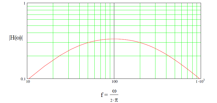
Therefore the attenuation through the filter at central frequency is exactly 2/3. So only 1/3 of the signal is left to be applied back to the input of the op-amp (OA). Thus the gain of the op-amp must be 3 to exactly compensate for it.
Note the phase at the central/resonant frequency is zero. So that the zero delay condition between the output and the feedback voltage is also met.
2. Low Distortion Oscillation
2.1 Conventional Wien-Bridge Oscillator
Continuing with the example above, at central frequecy the signal level at the bridge mid-point is 1/3 that of the output. So the gain applied by R2 and R4 must be at least 3 to maintain oscillation. At any other frequency the attenuation would be too much and oscillation would not occur. If the gain were greater than 3 then the signal level would grow until distortion occurred. Since distortion products would be more heavily attenuated through the R-C network further signal growth and distortion would be discouraged. Thus R4/R2 = 2 to just sustain oscillation.
It can be easily seen that the greater the gain then the greater the distortion will result. The fundamental signal level would still remain the same but all distortion products would be larger. For minimum distortion then the gain must be tuned to be as close to 3 as possible. Usually a resistance controlled by the output signal level is used for either R4 or R2 to accomplish this.
2.2 Balanced Wien – Bridge Oscillator
But there is more than one way to build the bridge. Instead of the first way which uses the output voltage to swing the top of the series RC pair positive and negative and then take 1/3 of that positive/negative signal to the opamp input, it can also be made with a second op-amp.
Here is a balanced version of the Wein Bridge oscillator [2]. The circled numbers represent nodes. Both op-amps have their inputs held near 0V to eliminate common-mode distortion within each. Oscillating output can be taken from node 4 or node 5:
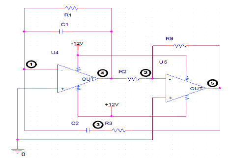
The math for this arrangement is similar to that of above. The two op-amp outputs operate in anti-phase with each other. As above, the resonant frequency is given by equation (11). Assuming again R1=R3=R and C1=C2=C, from the feedback filter analysis above it is directly derived that V4=-V5/2. So the magnitude gain of U5 needs only to be 2 to maintain oscillation. Thus R9/R2 = 2.
The key concept is the two op-amps drive the ends of the series-parallel string of RC pairs and holds the middle point at 0V. This does a very good thing: it prevents the input of either op-amp from being swung up and down. This is good since the bias currents, input impedances of those op-amps are a function of the common-mode voltage that they operate at. Changing input bias currents, etc. change the characteristics of the op-amp and this causes distortion. A small amount, but that small amount would prevent the oscillator from having distortion figures much lower then 0.1%.
A real implementation of the balanced Wien-Bridge oscillator can be found in this link.
Annex: OP-AMP Load Impedances
This is a simple calculation to show what the load on the op-amp would be. Assumes all the resistors and capacitors of the feedback filters are equal to R and C respectively.
A.1 Conventional Wien-Bridge Oscillator
The load impedance that the oscillator is working into can be expressed as follows. Here I assume that the R4, R2 combo represents neglible additional load:
\begin{equation} Z_o(s) = R + \cfrac{1}{sC} + \cfrac{R\cfrac{1}{sC}}{R+\cfrac{1}{sC}} = \cfrac{s^2R^2C^2 + 3sRC + 1}{sC(1+sRC)}\end{equation}
The magnitude of this load is:
\begin{equation} |Z_o(\omega)|= \cfrac{\sqrt{(1-\omega^2R^2C^2)+(3\omega RC)^2}}{\sqrt{(\omega^2RC^2)^2 + (\omega C)^2}} \end{equation}
At resonance:
\begin{equation} |Z_o(\omega)|\Bigr|_{\substack{ \\ \\ \omega_o = \frac{1}{RC}}} = \sqrt{\cfrac{9}{\cfrac{1}{R^2}+\cfrac{1}{R^2}}} = \cfrac{3R}{\sqrt{2}} \end{equation}
A.2 Balanced Wien-Bridge Oscillator
The load impedance that the balanced oscillator is working into can be expressed as follows. Here I assume that the R9, R2 combo represents neglible additional load:
\begin{equation} Z_{o4}(s) =\cfrac{R\cfrac{1}{sC}}{R+\cfrac{1}{sC}} = \cfrac{R}{1+sRC}\end{equation}
\begin{equation} Z_{o5}(s) =R + \cfrac{1}{sC} = \cfrac{1+sRC}{sC}\end{equation}
The magnitudes of these loads are:
\begin{equation} |Z_{o4}(\omega)|= \cfrac{R}{\sqrt{1+(\omega RC)^2}} \end{equation}
\begin{equation} |Z_{o5}(\omega)|= \cfrac{\sqrt{1+(\omega RC)^2}}{\omega C} \end{equation}
At resonance:
\begin{equation} |Z_{o4}(\omega)|\Bigr|_{\substack{ \\ \\ \omega_o = \frac{1}{RC}}} = \cfrac{R}{\sqrt{2}} \end{equation}
\begin{equation} |Z_{o5}(\omega)|\Bigr|_{\substack{ \\ \\ \omega_o = \frac{1}{RC}}} = \sqrt{2}R \end{equation}
Bibliography:
[1] Jim Williams, “Max Wien, Mr. Hewlett, and a rainy Sunday afternoon,” in Analog Circuit Design: Art, Science, and Personalities, Jim Williams, Ed. Boston: Butterworth-Heinemann, 1991, ch. 7, pp. 43–55.
[2] J. L. Linsley Hood, “New way of using Wien network to give 0.001% t.h.d” in Wireless World May 1981, pp 51-53
About the author:
B. Ap. Sci. (EE), 1977 University of Waterloo, engineer, entrepreneur, retired.
Subscription
If you liked this contribution, feel free to subscribe to our newsletter: