This article reviews the theory and implementation of the Bainter Notch Filter. Written and developed by Basin Street Design.
This calculation examines the effectiveness of a Bainter notch filter such as the Bainter circuit as seen in the figure below [1]. Low-pass, high-pass, and standard notch responses can be realized. The following picture shows the schematic of the circuit:
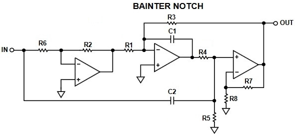
First, we’ll find the transfer function [2] in terms of the R and C values. Then, the notch filter design and tuning procedure is explined.
1. Bainter Notch Filter Block Diagram
The Bainter Notch Filter is composed of simple circuit blocks with one feedback loop and one feedforward loop. This circuit can be broken up into the gain blocks K1, K2, K3 and K4 and represented with the system architecture:
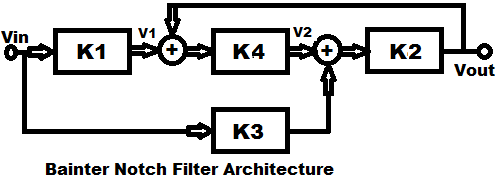
Where the different constant gains K can be calculated as:
\begin{equation} K_1=\cfrac{-R_2}{R_6} \end{equation}
\begin{equation} K_2=\cfrac{R_7+R_8}{R_8} \end{equation}
\begin{equation} K_3= \cfrac{\cfrac{R_5R_4}{R_5+R_4}}{\cfrac{1}{sC_2}+\cfrac{R_5R_4}{R_5+R_4}} \end{equation}
\begin{equation} K_4 =\cfrac{-1}{sC_1} \cfrac{\cfrac{\cfrac{R_5}{sC_2}}{R_5+\cfrac{1}{sC_2}}}{R_4+\cfrac{\cfrac{R_5}{sC_2}}{R_5+\cfrac{1}{sC_2}}} \end{equation}
K4 is multiplied by either 1/R1 or 1/R3 depending on the source of the signal through it, either V1 or Vout, respectively. Therefore, from the block diagram:
\begin{equation} V_{out} = K_2\left(\cfrac{K_1K_4}{R_1}V_{in}+K_3V_{in}+\cfrac{K_4}{R_3}V_{out}\right) \end{equation}
2. Bainter Notch Filter Transfer Function
Re-arranging for the transfer function yields:
\begin{equation} H(s)=\cfrac{V_{out}}{V_{in}} = \cfrac{R_3}{R_1}\cfrac{K_2(K_4K_1+K_3R_1)}{(R_3-K_2K_4)}\end{equation}
Substituting the K3 (equation (3)) and K4 (equation (4)) one at a time (using Mathcads symbolics “Substitute” command) and then simplifying with Mathcads “Simplify” function:
\begin{equation} H(s)= -R_3K_2R_5\cfrac{K_1-R_4s^2C_2R_1C_1}{R_1(R_3s^2C_1C_2R_4R_5+R_3sC_1R_4+R_3sC_1R_5+K_2R_5)}\end{equation}
Lastly, I assign this expression to H(s) after further manual simplification:
\begin{equation} H(s) = K_2\cfrac{s^2-\cfrac{K_1}{R_4R_1C_1C_2}}{s^2+\cfrac{1}{C_2}\left(\cfrac{1}{R_5}+\cfrac{1}{R_4}\right)s+\cfrac{K_2}{C_1C_2R_3R_4}} \end{equation}
The magnitude of the transfer function is:
\begin{equation} H(\omega)=H(s)\Bigr|_{s=j\omega} \end{equation}
\begin{equation} |H(\omega)|= K_2\cfrac{\left|-\omega^2 + \cfrac{-K_1}{R_4R_1C_1C_2}\right|}{\sqrt{\left(\cfrac{K_2}{R_3R_4C_1C_2}-\omega^2\right)^2+\left[\cfrac{\omega}{C_2}\left(\cfrac{1}{R_4}+\cfrac{1}{R_5}\right)\right]^2}} \end{equation}
The numerator of previous equation clearly indicates the existence of a notch frequency. The overall calculations and parameteres obtained from the transfer function are provided in next section.
3. Notch Filter Configuration
3.1 Notch Frequency
The magnitude function (equation 10) has a deep notch at the frequency where the numerator value goes to zero, given by:
\begin{equation} f_{notch}= \cfrac{1}{2\pi}·\sqrt{\left(\cfrac{|K_1|}{R_1R_4C_1C_2}\right)} \end{equation}
Additionally, the transfer function can be written as the canonical form of an active filter:
\begin{equation} H(s) = K\cfrac{s^2+s\cfrac{\omega_z}{Q_z}+\omega_z^2}{s^2+s\cfrac{\omega_p}{Q_p}+\omega_p^2} \end{equation}
Where:
· \footnotesize \omega_z is the frequency of the zero.
· \footnotesize \omega_p is the frequency of the pole.
· \footnotesize Q_z is the quality factor of the zero.
· \footnotesize Q_p is the quality factor of the pole.
Comparing equation (8) with equation (12) it can be derived that:
\begin{equation} f_{p}= \cfrac{1}{2\pi}·\sqrt{\left(\cfrac{K_2}{R_3R_4C_1C_2}\right)} \end{equation}
\begin{equation} Q_{p}= \cfrac{R_4R_5}{R_4+R_5}·\sqrt{\left(\cfrac{K_2C_2}{R_3R_4C_1}\right)} \end{equation}
3.2 Balanced Notch Filter
The DC gain and the high-frequency gain can be calculated as follows:
\begin{equation} |g_{DC}| = |H(\omega)|\Bigr|_{\substack{ \\ \\ \omega = 0}} = -K_1\cfrac{R_3}{R_1} = |K_1|\cfrac{R_3}{R_1} \end{equation}
\begin{equation} |g_{HF}| = |H(\omega)|\Bigr|_{\substack{ \\ \\ \omega\to \infty}} = K_2 \end{equation}
To obtain a symmetric notch filter, the low and high frequency gains must be balanced as shown below:
\begin{equation} |g_{DC}| = |g_{HF}| \rArr \cfrac{R_3}{R_1}=\cfrac{K_2}{|K_1|} \end{equation}
Note that once balanced the frequency of the notch (eq. 11) coincides with the frequency of the pole (eq. 13). For simplicity we will consider the following case:
\begin{equation} |K_1| = K_2 = 1 \rArr R_1 = R_3 \end{equation}
In this way the gain of the system is unity across all frequency except around the notch. And the bandwidth of the notch is given by the quality factor of the pole.
3.3 Frequency / Bandwidth Tuning
In the previous conditions, from equation 11, the frequency of the notch can be set with R3, R4, C1 and C2. Consequently, to change the frequency of the notch by 10:1 the value of any one of those must be changed by 100:1 or any pair by 10:1 each. Then, from equation 14, the quality factor can be independently adjusted with R5.
The following example shows the frequency tuning achieved with R4 in 10K steps:
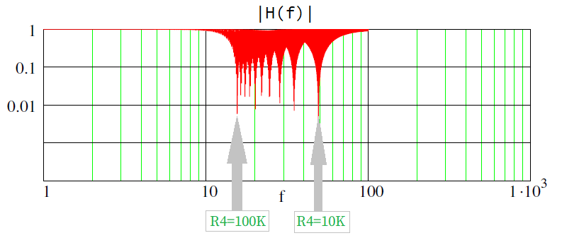
Note K1=-1, K2≈1.
R4 tuned from 100K to 10K in 10K steps.
The bandwidth of the notch is tuned with R5, as shown here:
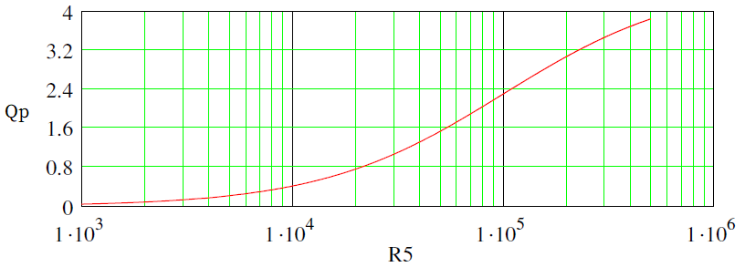
Obtained with the same values of previous picture for R4=100K.
The maximum achievable quality factor, associated to highest selectivity, can be derived from equation 14 assuming R5 tends to open circuit:
\begin{equation} Q_{p_{max}}=Q_p\Bigr|_{R_5\to\infin} = \sqrt{\left(\cfrac{K_2R_4C_2}{R_3C_1}\right)} \end{equation}
Hence, lower notch frequencies (higher R4) allow higher selectivity (higher quality factor).
4. Bainter Notch Filter Implementation
4.1 Schematics
This is the Bainter notch circuit schematics I built:
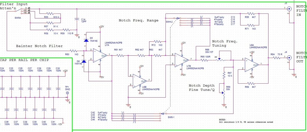
It includes a 0,-20, -40 dB attenuator on input, an input buffer and 75 Ohm output impedance to drive a 75 Ohm cable. There are four switched frequency ranges. The tuning pot is R66 (R4 above) and the Q pot is R69 (R5 above).
4.2 Prototype
4.2.1 Circuit
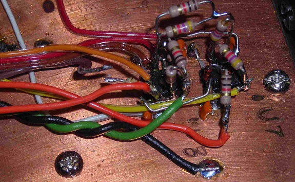
Now this is the Bainter circuit as built:
4.2.2 Test-Bench Bainter Notch Filter
Previous circuit was fixed inside a modded test-bench equipment, with the following front panel:
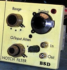
The range switch changes the frequency of the filter by decades while the 3-position input attenuation switch has positions for 0 dB, -20 dB and -40 dB attenuation. The small knob on that switch is the Q adjustment.
4.3 Performance
When swept by the spectrum analyzer the effect of the Q adjustment can be seen:
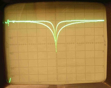
As advertised, the tuning of the notch is minimally affected by cranking it. Frequency is 0 to 1 KHz from left side to right.
It was just fine as is, so I leave that adjustment out completely since it serves no purpose to reduce the Q for my requirements. Namely, I used this Bainter notch filter to help measure the distortion of this generator based on the Wien-Bridge oscillator.
Bibliography:
[1] James R Bainter, Active Filter Has Stable Notch, and Response Can Be Regulated, Electronics, p 115-117, Oct 2, 1975
[2]: Nilsson, James, Electric Circuits, 2019.
About the author:
B. Ap. Sci. (EE), 1977 University of Waterloo, engineer, entrepreneur, retired.
Subscription
If you liked this contribution, feel free to subscribe to our newsletter:
