3.1 Integrated Circuits
In practice, the vast majority of professionals dedicated to electronics have neither seen nor fully understood what an electron is. They don’t need to, since they work at a much higher level. However, the electrical interactions of matter are the main field of study for professionals who are dedicated to the integration of electronic elements at their most physical level. This is fundamental task for the manufacturing of integrated circuits.
For example, due to the rise of digital microelectronics in all areas of life, it is essential to integrate components, especially transistors (component explained below), in the smallest possible space, which translates into higher processing capacity and lower power consumption. In this sense, some of the concepts typically heard in technology dissemination publications would be:
- Moore´s Law [1]: It’s a law formulated by a co-founder of Intel in 1965. It states that the number of transistors in a microprocessor doubles roughly every two years. This law has been complied with to date, which explains the immense computing capacity that is currently available with low energy consumption. The best example: the mobile phone that you have next to you on which you are perhaps reading this text.
- Nanometers: A nanometer (nm) is a very small length, specifically one billionth of a meter. That is, 1 nm = 10-9 m. If you take a meter and divide it into a thousand parts, you have a millimeter, and you can see what it measures on a conventional ruler. If you divide that millimeter into a thousand parts, you find a micron, and you can no longer see it. If you divide a micron into a thousand parts, then you have an nm. Every time a new family of processors is introduced, the announcement is accompanied by the nanometers (nm) used in manufacturing technology. This figure indicates the minimum length of the gate of a transistor, and therefore, the smaller that number is, the smaller the transistors and the better the technology. More transistors fit in the same space and also consume much less power. At the time of this writing, the most modern manufacturing technology is 5nm, and talk of 3nm is already beginning.
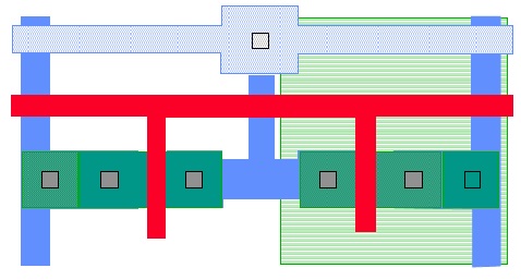
- CMOS Technology: CMOS stands for “Complementary metal-oxide-semiconductor” and it is the integration technology most used today to manufacture all types of circuits [2]. The substrate used is silicon [3], a semiconductor abundant in nature and cheap. That is why it is said that we currently live in the Silicon Age. And also for this reason the innovative region of California is called Silicon Valley, which is home to the world’s leading companies in the electronics and information technology sector. To continue lowering the nm of integration, at some point a substitute for silicon will have to be used.
Not always when speaking of integrated circuits, a level as low as that explained so far is implied. Furthermore, some professionals design integrated circuits by combining pre-engineered blocks, stages, and / or components for a given integration technology. It is also very common for an electronic engineer to design a product incorporating one or more integrated circuits and a multitude of discrete electronic components such as those described below.
Bibliography (Sponsored)
[1]: Wikipedia, Moore´s Law.
[2]: Razavi, Behzad, Design of Analog CMOS Integrated Circuits, 2016.
[3]: Wikipedia, Silicon.
<= Specializations in Electronics
Subscription
If you liked this contribution, feel free to subscribe to our newsletter:
