DIY Project: Redesigning and Building the Electronic Board of a Remote Control Car. Developed and written by Niva_v_Kopirce.
Christmas came and I was getting ready to give my nephew a cheap Chinese car. I always like to check beforehand if any gift containing electronic components works. It worked fine, however, I instantly noticed a few things that could be done better and/or upgraded.
The first idea was to add LED lights on the front and back. Since I already had clear plastic lights, adding LEDs and hot gluing them on was pretty easy.
The previous upgrade got me thinking about the capacity of the original battery pack. The original battery pack, consisting of 6 NiMH batteries, only had a capacity of about 700 mAh. Since six 1.2V rated NiMH batteries have 7.2V total, that’s about the same for two lithium-ion batteries in series. Fortunately, I had a lot of salvaged 18650s lying around and a few 16650s with a capacity between 2000 and 2300 mAh. The 16650s were almost perfect.
Why near perfect? Fully charged lithium-ion cells have about 4.2 V, giving 8.4 V total in series. Higher voltage means faster motors, but since the rotor is only a few coils it acts as an inductive load. And switching the inductive load causes voltage spikes – higher voltage means higher voltage spikes. Unfortunately, after some time, this led to burning out one of the four transistors on the original H-Bridge control board.
Although I replaced all the transistors with more powerful ones, added the missing flyback diodes and capacitors to reduce the voltage spikes (I will explain the reason for all this later), one transistor was still dying. So I decided to create a new control board with MOSFET transistors.
The content of the article is organized as follows:
1. How does a Remote Control Car work?
1.1 Transmitter
The principle lays in the term Remote Controlled, which suggests there is a remote controller often called transmitter. In layman’s terms, the transmitter converts the human signal (acceleration, steering) into electrical signals, which are transmitted by radio frequency (RF) to the car’s receiver.
Typically the transmitter also performs the following functions:
- The human input signals are usually modulated or encoded so that the transmission does not interfere with signals from other controllers.
- This signal is often divided into channels, where each channel is for a different input: one channel for forward, one for reverse, another channel for left or right and more advanced RC cars have transmitters with even more channels.
1.2 Control Strategy
Depending on the system, there are simple controls and advanced controls. Simple controls only send ON/OFF (HIGH/LOW, 1/0) on each channel, so the car moves at full speed or not at all. Advanced systems used in more expensive commercial products offer a wide variety of transfer protocols, each of which operates differently.
For example, advanced systems can use any of the following control strategies:
- The analog protocol called pulse width modulation (PWM) uses a different duty cycle (duration of a HIGH pulse in a period) to determine speed or slew rate; the disadvantage can be the need to use one channel per input signal.
- Another analog option is pulse position modulation (PPM), which combines the PWM pulses from each channel one after the other into a single signal.
- Digital (serial) protocols would be, for example, i-BUS or s-Bus, which send digital values.
1.3 Motor Control
The last step, after the receiver receives and distributes the signals on the corresponding channels, is to control the motors. Depending on the complexity, there are brushed DC motors, brushless DC motors (BLDC) or servo motors:
- The brushed DC motor requires only a simple controller consisting of a transistor, or for the option of driving the motor in both directions, the so-called “h-bridge”.
- The BLDC motor, since it is usually a three-phase DC motor, requires an electronic speed controller (ESC).
- For servo motor steering, a dedicated servo motor controller is needed.
This project is aimed at a simple remote control car controlled with brushed DC motors, IC controller for steering and h-bridge for propulsion.
2. Reverse Engineering the Original Remote Control Car Board
Obviously, in order to keep the original controller board, it is necessary to preserve some original components of the remote control car as well.
2.1 List of Materials
The car’s controller board consists of these components:
- 3V3 LDO Regulator, SOT-23-3 pack (LDO stands for Low Drop Out) to lower the battery voltage to a stable 3.3V to power the receiver IC.
- Unbranded Chinese receiver IC operating at 2.4GHz, SOP-16 package.
- 12MHz crystal oscillator to provide the clock signal for the receiver IC.
- MX08E motor controller for the steering motor, SOP-8 package.
- 4x BJT transistors (2x NPN, 2x PNP) in H-bridge arrangement for forward/reverse drive.
- Other passive components, mainly capacitors for filtering or resistors for feedback.
- Antenna.
There were also two transistors in SOT-23-3 package whose exact purpose I haven’t figured out, but I suppose they could have been there as AND gates to drive the bases of the h-bridge transistors.
2.2 Key Components
The components needed for reuse are the LDO regulator, the receiver integrated circuit, the motor controller and capacitors whose values I have not been able to determine.
By measuring and tracing around the original board, I was able to determine the following pinout for receiver IC:
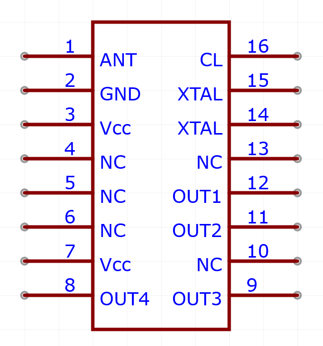
When pushing trigger for going forward, OUT1 outputs voltage; for going backwards, OUT2 outputs voltage; OUT3 and OUT4 are for right and left respectively.
The steering motor driver marked as MX08 was easy to pinout. Since it had only 8 pins: two inputs, two outputs, two pins for ground, one power source input and a last unidentified pin connected to a voltage divider.
On the other hand, tracing the LDO regulator was pretty straightforward.
That’s all there was necessary to back trace.
3. New Remote Control Car Board Design
When it is clear how the original board works, it is relatively simple to design a new one. And since it is intended to replace the original transistors with MOSFETs, it is a good idea to test whether the envisioned configuration will work. The design was divided into three parts: testing on the breadboard, creating the schematic, and fabricating the new PCB.
3.1 Remote Control Car Board Prototype
3.1.1 MOSFETs
3.1.1.1 Fundamentals
Let’s start with some theory. MOSFET is short for Metal Oxide Semiconductor Field Effect Transistor. Like most BJT transistors, it has three terminals, but here they are referred to as source, drain and gate. MOSFETs are often used as switches because of their switching speed.
Their operating principle is quite simple. Closing a switch typically means closing the circuit so that current can flow. The same is true for the MOSFET: applying voltage to the gate terminal is the same as pushing a button. When sufficient voltage is applied (above the threshold level, which can be found in the data sheet usually as VGS(th)), current flows from the drain to the source. However, this only happens with N-channel MOSFETs (N-MOS). Everything is the other way around for P-channel (P-MOS). When ground is connected to the gate terminal, current flows from the source to the drain, so the voltage applied to the gate terminal causes the P-MOS to close.
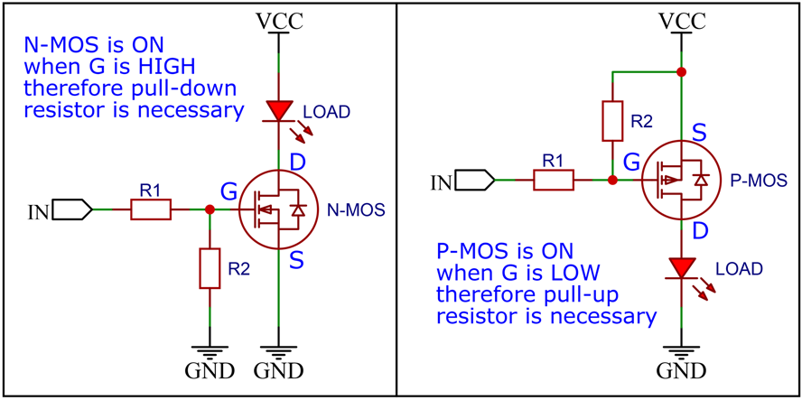
The previous picture summarizes the content of this subsection. To distinguish the schematic of a MOSFET, the N-MOS has an arrow on the inner side of the gate and the P-MOS has an arrow on the outer side.
3.1.1.2 Gate Voltage
While the base of the BJT transistor operates on current, the gate of the MOSFET operates primarily on voltage. One important thing to keep in mind when working with MOSFETs is the floating gate. The floating gate means that when the gate is not being driven, it picks up ambient noise, which causes the MOSFET to not function properly.
A simple solution is to add a pull-up/pull-down resistor. For the N-MOS, a pull-down is used (R2 in the picture above, left), so when the gate has no voltage, it has to be tied to ground, therefore, the transistor remains closed. The P-MOS uses a pull-up (R2 in the picture above, right), connected to a voltage higher than the threshold voltage.
3.1.1.3 Low/High Side Switching
The N-MOS has the load connected to the supply voltage and the source to ground; this is called low-side switching because the switch, N-MOS in this case, is on the low side of the load.
On the other hand, P-MOS uses high-side switching. It is the most suitable configuration, this goes down to the basic rules of Kirchhoff’s laws. Since the threshold voltage, which determines whether the MOSFET opens or not, is given by the voltage difference between the gate and the source (VGS(th)), putting the load on the low side means that the voltage difference between the gate and the source might not exceed VGS(th).
3.1.1.4 Protection
The resistance (R1) between the input signal (IN) and the gate is a protection. We know that in the real world no component is ideal. In this case the transition between the gate and the source has input capacitance, in other words, it acts as a capacitor. When connecting the capacitor to the voltage, the instantaneous load causes instantaneous current consumption. It is a brief peak current draw until the capacitor is charged. However, this brief current spike could damage the microcontroller. The resistor is there for protection.
The gate draws almost no current (as stated above, no component is ideal), therefore there is almost no voltage drop across this resistor and that is why it has almost no impact on the gate conduction.
3.1.2 H-Bridge
3.1.2.1 Fundamentals
The ideal H-bridge component is the MOSFET. And the H-bridge is the ideal circuit for controlling motors. Switching or driving the motor is relatively simple: just a MOSFET to turn on the motor or a PWM (a MOSFET is also often used) to control the speed. However, driving the motor in the opposite direction is a problem. DC motors need to reverse polarity to rotate in the opposite direction. This is not possible with one or two MOSFETs.
The basic H-bridge configuration is shown below. For simplicity, 4 switches have been used:
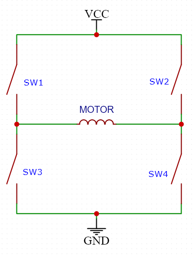
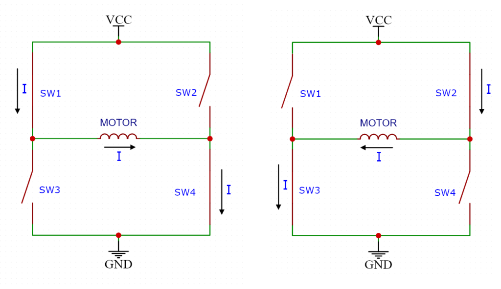
Closing SW1 and SW4 creates path for current in one direction. If SW2 and SW3 are closed, current will flow in opposite direction. It is crucial to open the other pair of switches to avoid short circuits. If SW1 and SW3 were closed at the same time, current would flow this way and since the resistance there is very small, the current would be too high and destroy the transistors acting as switches.
In real applications MOSFETs are used instead of switches. Sometimes complete integrated circuits are used as H-bridges, but the principle is the same.
3.1.2.2 Protection
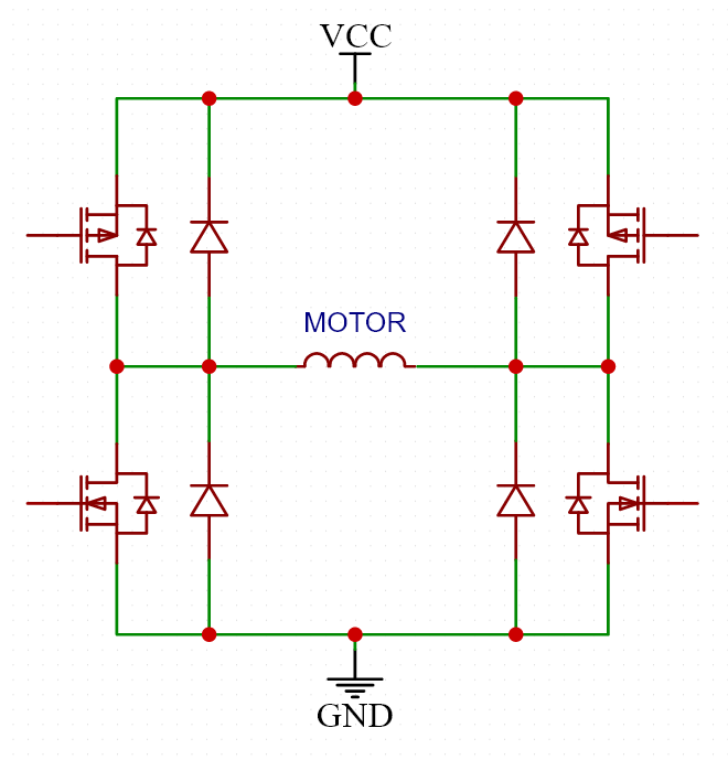
To complete the whole H-bridge, one more thing is missing. When the inductor is disconnected from the current source, the magnetic field collapses and the stored energy must be released somewhere. The collapse of the field creates a current flowing in the opposite direction and is called flyback. This occurs when the direction of rotation is reversed or when the push button is released.
The aforementioned voltage spike could damage the transistors, so diodes are used to prevent this. Each diode is reverse biased, so the top diodes have cathodes connected to the voltage source and the bottom diodes have anodes connected to ground. The following picture shows a complete H-bridge with flyback diodes. Note how the P-MOS is used as a high switch and the N-MOS as a low switch.
3.1.3 Testing on Breadboard
The time has come to practice. Before designing a new PCB (printed circuit board), testing the prototype circuit is useful to overcome possible problems. To test prototypes, I use breadboards. The breadboard is a perforated plastic board usually consisting of 63 rows by 2×5 columns of holes with spring clips inside, always connecting one row on each side. Using breadboard is good for simple projects like this one. It is not recommended to use breadboard for high frequency circuits. Spring clamps on breadboard have parasitic characteristics such as high capacitance, inductance and impedance, for example, which, when using higher frequencies have a large unwanted impact on the circuit. For higher frequencies, it is better to use a perfboard and solder directly to it. Fortunately, this is not a problem for this H-bridge.
3.1.3.1 Connecting to the Remote Control Car Receiver
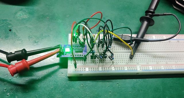
The first step was to create the H-bridge on the breadboard and test if it works correctly and changes polarity as desired. Then I used the RC car receiver, soldered it to the PCB adapter from SOP-16 to 16 DIP (Dual In-Line Package – pins, in my case) and tested my H-bridge with the original RC receiver. In the image below, although not clearly visible, is the breadboard with the H-bridge circuit, connected to the oscilloscope.
3.1.3.2 Connecting to the Remote Control Car Motor
The circuit worked as expected, however, with the original motor connected, it revealed a problem. The problem was voltage spikes around 19V when the motor was spinning. As mentioned, the flyback diodes are there because of the collapse presented in the motor coils, but the rotating rotor made of coils, inside the stator made of magnets causes these voltage spikes. A simple way to avoid this problem is to add capacitors from the motor terminals to ground. The capacitor functions as a filter in this case. The frequency of these spikes could be used to calculate the value of the capacitor, but I tried 100 nF capacitors and it worked as expected. Unfortunately, I did not save the oscilloscope capture, so there are no pictures.
3.2 Remote Control Car Board Schematic
When the prototype circuit works, it is time to design the schematic and then make a printed circuit board. For the schematic design, the online PCB design tool EasyEDA was used. It is a good practice to divide the schematic into separate blocks to make the schematic easily readable and synoptic.
3.2.1 H-Bridge
The final H-bridge looks as depicted below.
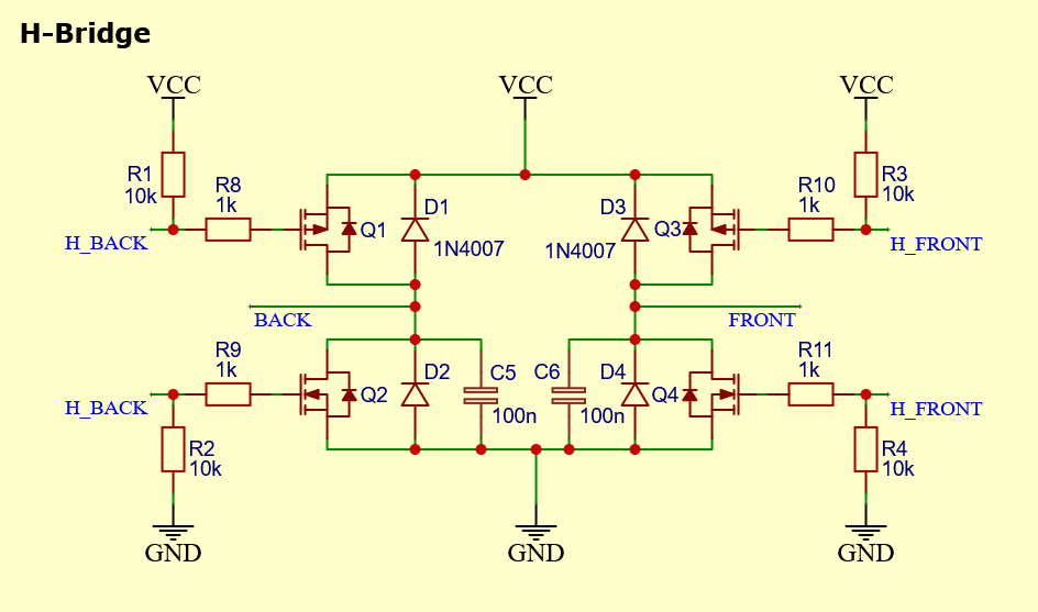
The apparently disconnected cables are at the ends labeled with network tags (blue). These network labels tell the editor which cables/traces to connect, even though they are not physically connected in the editor. This feature helps to make the schematic more organized. It works the same as the VCC and GND symbols.
The BACK and FRONT labels are connected to the motor output connector. H_BACK and H_FRONT are connected to the RC receiver. When the forward push button on the transmitter is pressed, the H_FRONT signal is at logic LOW level (GND) causing Q3 P-MOS to open and keeping Q4 N-MOS closed. Simultaneously H_BACK is at logic HIGH level, causing Q1 P-MOS to close and Q2 N-MOS to open, so current flows in the direction of the FRONT to BACK tags/terminals. When the BACK (reverse) button is pressed, the situation is vice versa and current flows from the BACK to the FRONT labels/terminals.
3.2.2 Integrated Circuits
Integrated circuits are copied from original control board. Their schematic is depicted below.
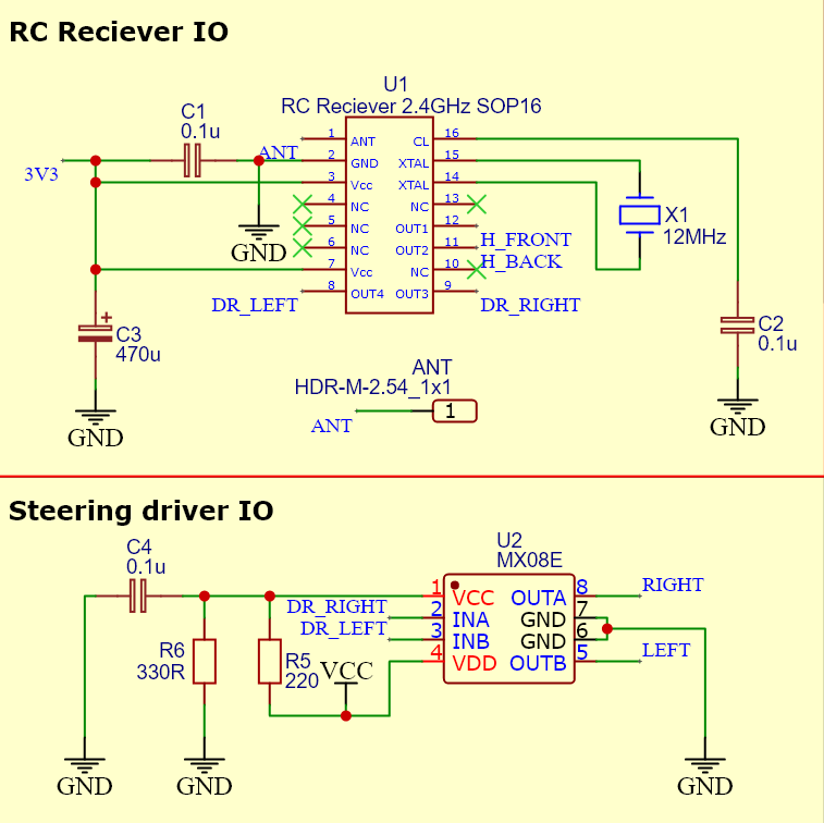
Here we can see the H_FRONT and H_BACK nets connected to the RC receiver U1. The DR_LEFT and DR_RIGHT nets are connected to the U2 IO driver for steering. The green “x” symbols on the RC receiver pins tell the editor not to connect those pins. They are not necessary, but when generating the PCB from the schematic there will be no warnings that some pins are not connected.
The U2 symbol was taken from the EasyEDA user contribution library and in this case the VCC and VDD pins are misleading. For this purpose, it is sufficient and I decided to use it anyway. The resistors R5 and R6 are original, and since the MX08E has no datasheet, their purpose is unknown.
For the antenna I used a separate header pin, this creates a hole in the PCB to solder the antenna.
3.2.3 Rest
Last things on schematic are the 3V3 LDO regulator and the connectors.

3.3 Remote Control Car PCB Design
3.3.1 Summary
EasyEDA automatically converts the schematic on the printed circuit board. By “automatically converts” we mean converting the schematic symbols of the components into physical components with their corresponding footprint. The traces are not yet generated, because each component must first be moved into its place.
So far the components are connected through networks called ratlines. There are two ways of routing (creating physical traces from the networks connecting the components): autoroute or manually. Autoroute creates traces automatically, but is limited by established rules, not always reliable.
I recommend routing the traces manually, it is a more reliable method. The manual method occupies the mind, it makes one think about placing each component. Of course, it takes a few tries until it is perfect. Normally, I route everything except ground grids, the reason being that for ground I use ground plane. First, it reduces noise generated by high currents and high frequency signals, second, it saves toner and etching solution (to be mentioned later).
3.3.2 AutoPlace
The image below shows the components automatically positioned by EasyEDA and connected by blue lines.
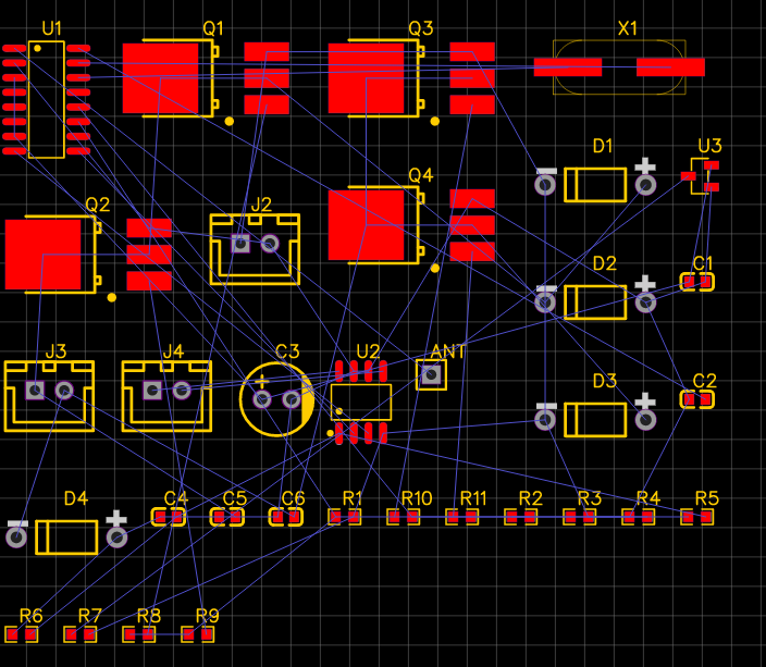
The red rectangles correspond to the top copper layer of a printed circuit board, while the yellow lines are the outlines of the components. If there are parts placed on the bottom layer, the color would be blue for the copper traces and green for the outlines of the components. In addition, the gray circles are the pads of the top and bottom layers, called multilayer.
It is important to keep components with more than three terminals on the same layer as the rest of the component, otherwise the trace would be mirrored.
EasyEDA also generates the board outline which is purple, I usually remove the board outline as it is not necessary.
3.3.3 HomeMade PCB constraints
When building a DIY PCB, the physical board to be etched must be considered. The main factors are the number of layers and the size. The control board will be single sided. As for the size, I have a 10×10 cm FR4 (0.6 mm epoxy) sided PCB that will be cut to the desired size.
For the design of the PCB size I always try to design the smallest possible PCB taking into account all the necessary factors, such as heat dissipation, for example.
3.3.4 Place & Route
Connectors and all THT (through hole technology) components are placed on the bottom layer without copper. All SMD (surface mount device) components are left on the top layer.
In practice, the layer without copper faces up, ergo it should be called the top layer, and the side with SMD components faces down, ergo it should be called the bottom layer. However EasyEDA by default uses red as the top layer and because I have most SMD components, I refer to copper layer with SMDs as the top layer.
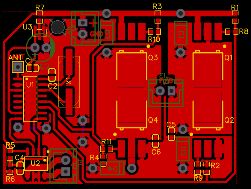
The picture above shows the final PCB layout.
- The MOSFETS were placed on common copper pads, so that they dissipate as much heat as possible, but also take up as little space as possible.
- Placing decoupling capacitors (C1 and C4) closer to the voltage input pins is vital, otherwise they lose their purpose.
- Two jumpers were also necessary to connect ground planes (2 multilayer pads below U1 and two perpendicular ones further to the right, connected by blue trace).
- For signals with higher currents, wider traces are needed. The trace width can be calculated online.
3.3.5 Home Made PCB
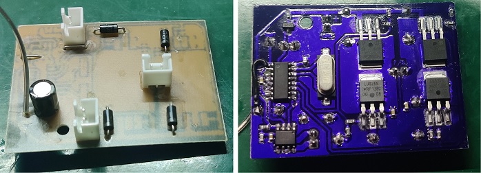
The PCB was manufactured and populated following the procedure described in the annex at the end of this article. The following pictures shows the obtained results.
4. Upgraded Remote Control Car
4.1 Probing, Testing and Assembling
Before placing the control board in the remote control car, there is one last step and that is to test the functionality of the board.
First inspect if there are no errors in component placement, then the electrical functionality. By measuring the resistance of the input voltage connector, we can make sure there is no short circuit or too low resistance.
If the resistance is reasonably high, the next step is to connect the control board to the bench power supply and check the current consumption, which should not be too high or zero.
When the current is correct, the next step would be to measure the correct output voltage of the LDO regulator. If the LDO regulator produces the desired voltage and the input voltage of the remote control car receiver IC is correct, it is time to test the nominal functionality.
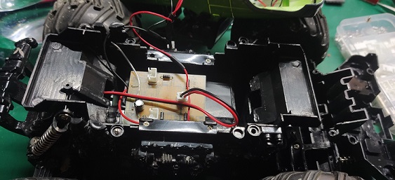
Now connect the output connectors for the motors to the oscilloscope. When pressing the forward or reverse button on the remote control, there should be corresponding signal changes. The working control board is placed in the remote control car and tested. When everything works as expected, the remote control car is assembled.
4.2 Results
Finally, this video shows the remote control car working as expected:
A. Annex: Remote Control Car Home Made PCB Manufacturing
When PCB design is finished, it’s time to create it. I use photosensitive dry film for manufacturing PCBs (other method for instance is heat transfer by ironing the toner printed on a photopaper onto the copper). For this method following tools/devices are needed:
- Laser printer (the highest the resolution the better)
- Transparent sheet for laser printer
- Some software for editing PDFs (Photoshop is used, GIMP may be used as well)
- Photosensitive film (negative)
- UV Light (395 – 405 nm, I prefer UV LEDs)
- Two sheets of glass
- Laminator (usually format A5 is sufficient, but A4 is more available)
- Etching solution (Ferric chloride Fe2Cl or sodium persulfate Na2S2O8)
- Negative developer solution (Sodium carbonate Na2CO3, also known as the soda ash)
- Chemicals for cleaning (Acetone, Sodium hydroxide NaOH)
- Sandpaper
- Plastic containers for chemicals
Other tools are optional for soldering SMDs:
- PTC heating plate
- Solder paste
- Aluminum can
Creating the PCB is divided into 8 phases:
- Printing a design mask
- Preparing a copper layer of the PCB
- Transferring mask onto the copper
- Developing the mask
- Etching and cleaning PCB
- Creating a protection layer
- Making Stencil
- Populating the PCB
A.1 Printing Design Mask
A.1.1 Export Files
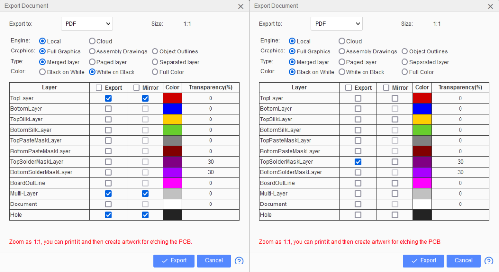
The PCB design is exported in PDF or SVG format. The design has to be exported as negative, white on black and mirrored. In EasyEDA this is done in the following menu: File > Export > PDF (SVG). In the export window select White on black, TopLayer, MultiLayer and Hole, all mirrored and click Export.
Then TopSolderMaskLayer is exported as well, black on white, not mirrored, which will be used for the protection layer and finally edited for the stencil mask.
A.1.2 Edit Files
The exported files are edited in Photoshop with the highest possible resolution (be careful, temporary files take up a lot of disk space, I use 4200 DPI). The resolution is noticeable on the transparent sheet.
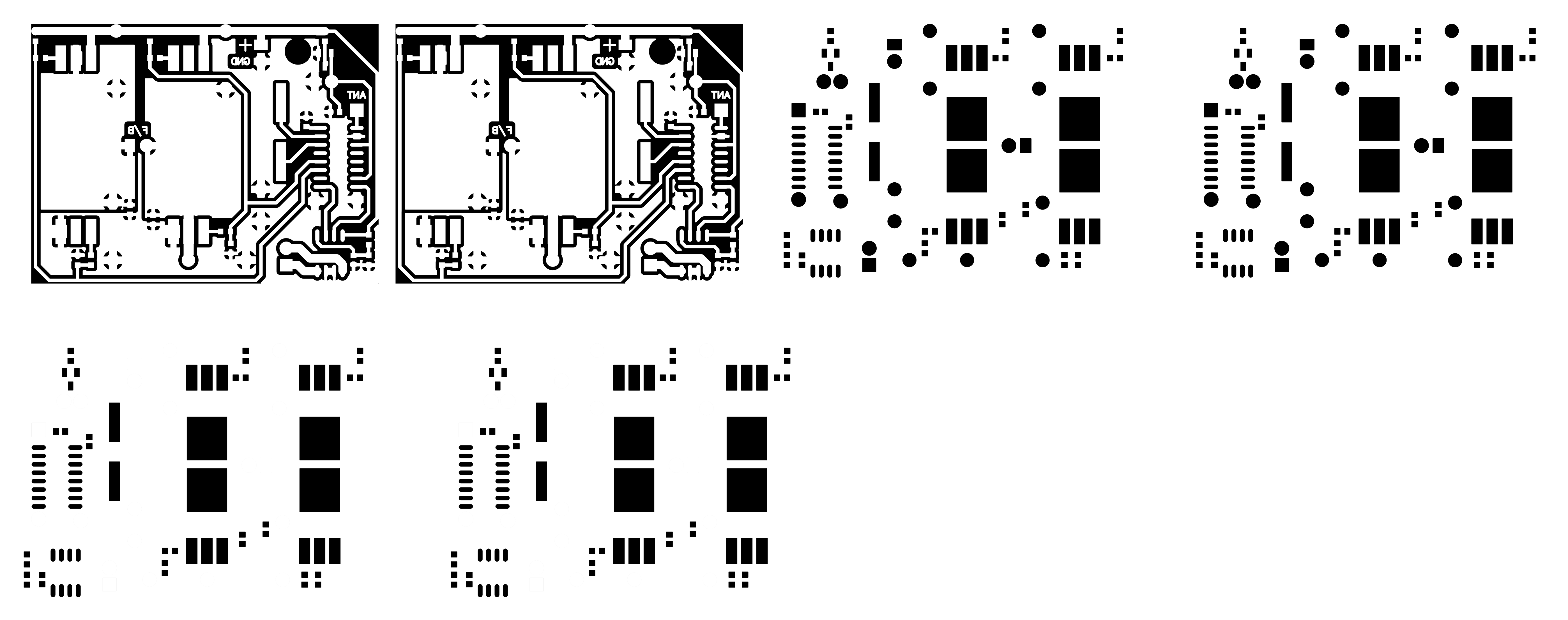
Printing on the transparent sheet requires two layers of the negative mask, otherwise the UV light will pass through only one layer. (It is possible to print on tracing paper, unfortunately, I have not been able to achieve good results, although I have not spent too much time on it). Two copies of the negative of the PCB layout are placed adjacent to each other.
Finally, the solder mask layer is duplicated in the photoshop file of the PCB layout and two copies are made as well. The optional stencil also uses solder mask, however some unnecessary pads have to be removed, I keep only those pads to which I need to apply solder paste (SMD components).
The final edition is shown below:
A.1.3 Results
The fact that dry photosensitive negative film is used makes it necessary to use negative for printed circuit board design. The rule is that what is exposed to UV light sticks to the copper, and what sticks to the copper does not etch. Therefore, traces and pads should be white on the design, so that they do not etch. When used with ground planes it also saves a lot of toner and less etched copper means more use of an etch solution. The same goes for the protection layer and the stencil, the only thing to mask are the pads.
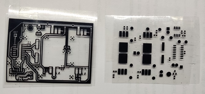
After printing, each pair of blocks is placed on top of each other and taped together to form a perfect mask. The printed toner layer should face downwards.
A.2 Preparing a Copper Layer of the PCB
First the laminator is heated, which saves time. In order for the dry photosensitive film to adhere well to the copper, the copper must first be cleaned. A good option is to use water-based sandpaper, grit around 800-1000, then sand it under hot water, especially around the edges, then wipe it with aceton and kitchen paper to remove any remaining grease and dry it. Next dry the copper carefully, avoiding touching it with your fingers.
The dry photosensitive film has three layers. The upper matte film, the intermediate photosensitive film and the bottom glossy protective film. To stick the film to the copper, the matte film is removed. Pressure is applied from the center of the PCB towards the edges to avoid bubble formation.
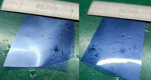
When the laminator is heated, the printed circuit board with the film is placed between the folded paper, this is to prevent the photosensitive layer from sticking to the heating cylinders (don’t ask me how I know this). The heat from the laminator and the pressure causes the film to shrink and stick to the copper. Finally, using masking tape, the printed PCB mask is placed over the film, shiny side up, so that the text is legible (not reflected).
It is also advisable to expose the dried film to as little light as possible before curing under UV light.
A.3 Transferring mask onto the copper (UV Curing)
For UV curing 4x3W UV leds (400-405nm, 140° cone angle) are used. They are at a distance of 10 cm from the cured board, and 10 cm from each other.
The printed circuit board is placed between two sheets of glass, so that the printed negative is pressed as close as possible to the dry photosensitive film.
Curing takes 2 minutes and 45 seconds to 3 minutes. The curing time depends on the power and distance of the UV light used; also, if tracing paper is used, it may take longer to transfer the mask correctly. The crucial step after curing is to let the polymerization do its work and let the cured PCB rest for at least 15 minutes, cured side down to protect it from any additional unwanted UV light. After additional polymerization, the contrast should be higher and the cured film will adhere better.
Always wear UV protective goggles when working with UV light.
A.4 Developing the Mask
During the polymerization rest, the negative developing solution is prepared. I use sodium carbonate (Na2CO3), known as soda ash, in a 1:10 ratio with distilled water. For 200 ml of distilled water, 20 g of Na2CO3 is used. For long-term storage, it is convenient to use a sealed plastic container. The concentration decreases with use, but so far my first batch has developed tenths of PCBs in half a year.
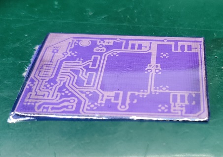
To develop the photosensitive layer, the glossy protective layer must be carefully peeled off. The printed circuit board is not immersed in the solution, but brushed with a brush soaked with developing solution. The uncured film will react with the developing solution, creating a whitish layer; after a few minutes of brushing, the photosensitive layer disappears. Once the film has been developed, it is necessary to wash off the residue with water, preferably using a soft toothbrush. If any trace is damaged (such as the trace at the bottom center of the PCB), it can be fixed with 0.3 mm waterproof permanent marker.
A.5 Etching and Cleaning the PCB
There are several methods to etch a copper printed circuit board. Either using ferric chloride, which can leave a mess if not used carefully, or hydrochloric acid mixed with hydrogen peroxide accelerated with electrolysis (however hydrochloric acid is highly corrosive and caustic), or using heated sodium persulfate, which seems to be the cleanest and safest method. However, always wear nitrile gloves and eye protection when handling chemicals.
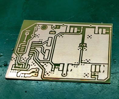
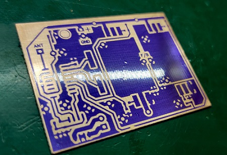
To prepare the etching solution with sodium persulfate, mix 20 g of persulfate per 100 ml of water. A reasonable etching time requires heating the solution to 40-50°C. The etching process takes 5-10 minutes, although a stronger solution may speed up the etching time. Etching is performed when no copper stains are exposed. After etching, the photosensitive film must be removed. To do this, soak the etched plate in a sodium hydroxide (NaOH) solution for a few minutes and then rinse it with tap water. Now is a good time to drill holes if necessary. The etched PCB is shown in the image above. The slight oxidation is caused by leaving the PCB too long in the sodium hydroxide solution, this can be removed by sanding the board a little.
Before placing the optional protective film or components on the etched PCB, it is good practice to probe the traces to make sure there are no shorts between them or interruptions. If all is well, let’s continue.
A.6 Creating a Protection Layer
This step is optional, but it protects the copper traces from oxidation. Another option would be to use liquid tin and dip the PCB in the liquid tin for a few seconds, the tin layer does not usually oxidize. However, a disadvantage of tinned PCB is when using SMD components, also the price of liquid tin is not worth it. The protective film helps to avoid bridges when soldering components with solder paste and thermal plate.
Photosensitive dry film usually cannot withstand too high heat, but it is a reasonable diy solution. In industry, a UV-sensitive paste is often used that is spread on the PCB and then exposed to UV light for a few minutes. In a hobby environment, this method is cumbersome and does not produce satisfactory results due to the uneven distribution of the paste, but on the other hand it is more durable and can withstand more heat than dry film. There are a few other options as well, but I focus on this inexpensive diy method of using dry film.
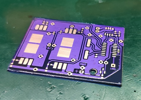
The process of making the protection layer is the same as for etching the PCB, so I will be brief. First step is to clean the PCB with sandpaper and aceton. The second step is to stick the dry film to the PCB. Next, after letting the PCB go through the laminator, put the printed solder mask on top and expose it to UV. After letting the polymerization do its thing, peel off the protective film and finally develop in sodium carbonate. The additional UV exposure should make the film more durable.
A.7 Making a Stencil
A.7.1 Stencil Plate
At this point the PCB is ready to be populated with components. But soldering SMD components with a regular soldering iron can be a challenge for beginners and requires some skill.
The most convenient is to use solder paste and let the heat plate do the work. But solder paste is annoying to work with, without the use of dispenser and even then, it can be nightmarish, when the solder paste does not stay on the copper pads, but everywhere.
In the industry a stencil plate is used, which is a thin steel sheet (from 0.05 mm to 0.3 mm) with etched holes. On this steel foil the solder paste is spread, resulting in the desired amount of solder paste on the copper pads.
In a hobby environment we can use almost the same technique although instead of using steel we can use an aluminum can, from a beer can for example. By cutting off the top and bottom and cutting the rest in half we get a fairly useful amount of aluminum foil for the jig. The inside of the can is coated with a film of epoxy and the outside has paint on it, both of which must be removed. To remove the paint and epoxy, acetone is effective only after preheating the aluminum foil.
A.7.2 Procedure
The creation of the stencil for the solder paste uses the same method as for the creation of the PCB, except that instead of using sodium persulfate for etching, heated ferric chloride must be used. For the mask, the exported EasyEDA paste mask layer is used.
The rest of the approach is as mentioned above, i.e. clean the aluminum foil with acetone, glue the dry foil onto the foil, use the laminator for better adhesion, cover the printed masks with transparent foil, expose to UV, polymerize, develop and etch. For etching it is convenient to cover one side with adhesive tape, or optionally leave the epoxy layer on the film and remove it later.
The image below shows the stencil obtained.
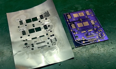
A.7.3 Spread the Solder Paste
To spread the solder paste over the stencil, the PCB must be fixed together with the stencil. In the picture below you can see the gap between the PCB and the stencil caused by the edges of the stencil sticking to the desk causing the stencil to curve upwards. It is not a big problem, however, a more convenient method is to use some unused PCBs (of the same thickness), put them around the etched PCB and tape them together.
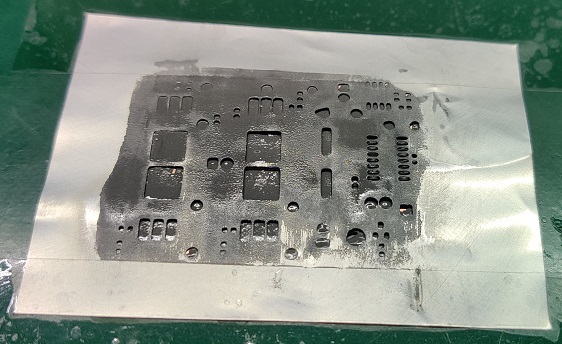
And the general rule of thumb is the less solder paste, the better. When too much solder paste is applied, small components like resistors, for example, tend to lift, or the solder paste makes large solder blobs, making it harder for the components to stay in one place or realign with the pads. An old credit card, squeegee or anything flat and hard can be used to spread the solder paste.
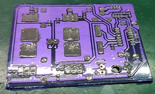
After carefully removing the stencil and cleaning the PCB with isopropylalkohol, the PCB can be populated with components.
A.8 Populating the PCB
It is recommended to populate the PCB with solder paste applied as soon as possible. Always starting with the smallest components, because when the big ones are already there, it is very uncomfortable to manipulate with the small ones.
Once populated, it is time to preheat the hotplate and reflow, which is to melt the solder paste in the solder. When buying solder paste from a reliable source, the recommended reflow curve or profile should always be included and following it produces the best result.
If you buy cheap solder paste from aliexpress or a similar source, it will work in any case, but by placing the etched and populated PCB on the heat plate before it reaches its maximum temperature, you make sure to avoid any temperature shock. The same goes for cooling the finished reflow, to avoid any thermal shock cooling the PCB should be done slowly.
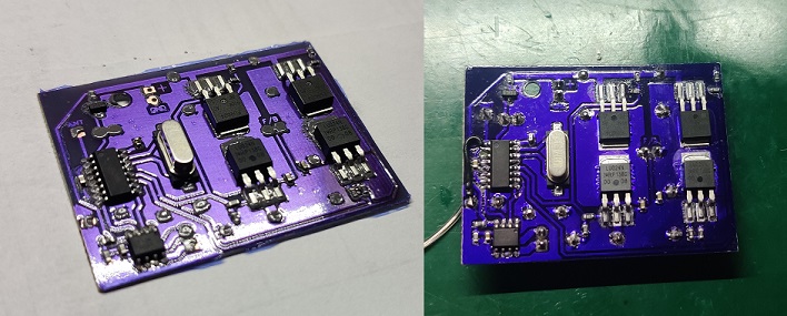
Shown below is the PCB populated before reflow and the nearly finished PCB after reflow. During the reflow the protective dry film will get darker and more adhesive but brittle due to high temperature. After populating the other side of the PCB, the control board is done.
Subscription
If you liked this contribution, feel free to subscribe to our newsletter:
